
Digital Logic Circuits
Start with digital signals and logic gates such as AND, OR and XOR, then design combinational circuits, latches, flip-flops, counters and state machines. Connect truth tables, equations, circuits and waveforms directly, and verify your designs in RTL labs. The optional advanced chapters extend the course to datapaths and interfaces.
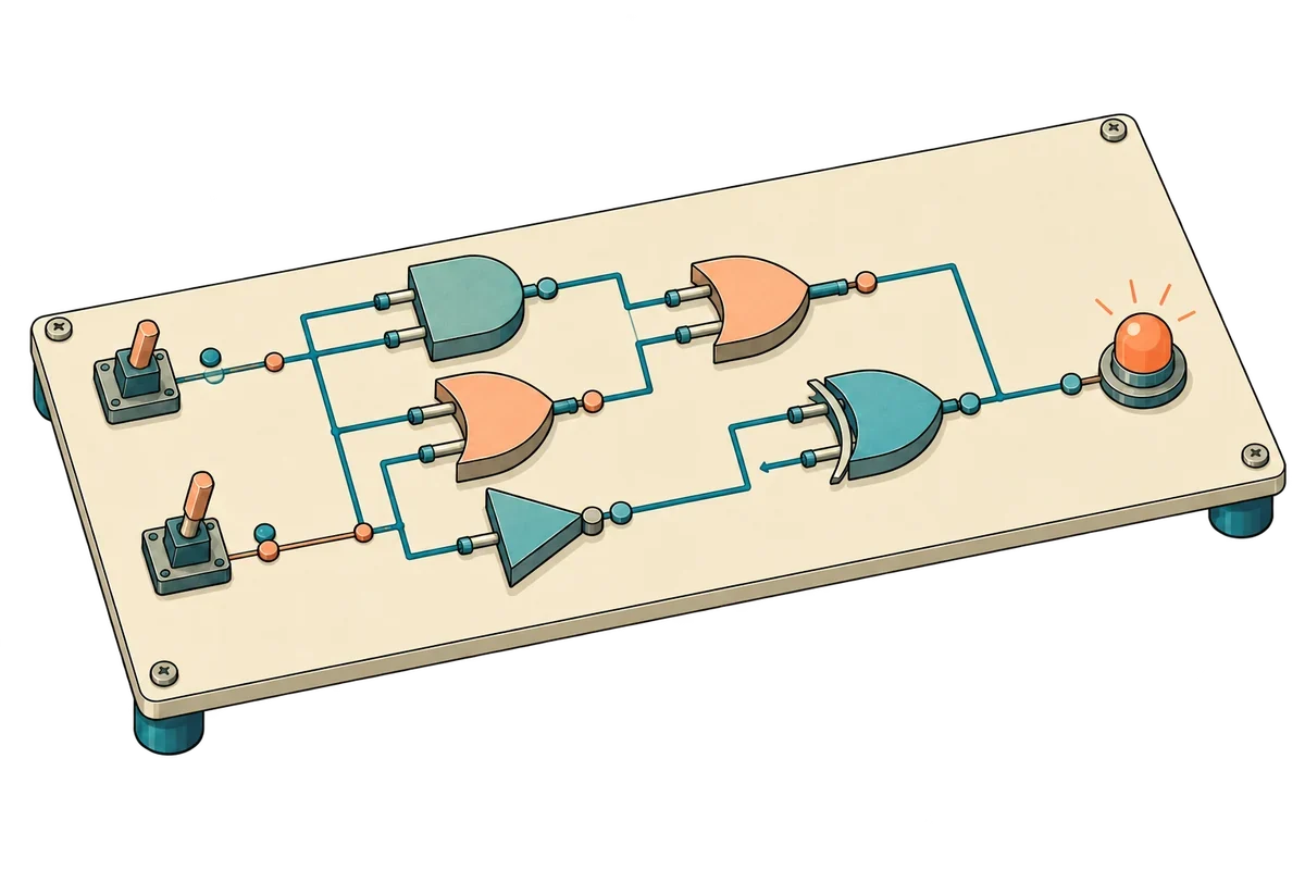
What you will learn
- Distinguish logic values from voltages, and explain the truth tables, symbols and equivalent circuits of eight gate types.
- Design combinational circuits from specifications using SOP, POS and Karnaugh maps, and test every input combination.
- Define input conditions and boundary cases for encoders, decoders, multiplexers, demultiplexers, adders and comparators.
- Explain how latches differ from flip-flops, and design the update rules for reset, enable and clock.
- Implement counters, shift registers and state machines in RTL, and analyze timing, asynchronous inputs and debouncing.
- Verify designs with independent reference models, and complete an overlapping 101 pattern detector.
- Extend these foundations to ALUs, memory, FIFOs, pipelines and interfaces in the optional advanced chapters.
Before you begin
These browser exercises use educational models; they do not compile or run HDL. To run the supplied source separately, follow the Digital Design Studio guide for your operating system and sign in when the operation requires it.
Installation and first launch ↗ · Downloads ↗Curriculum
- Digital signals and number representations
- Digital signals: when voltages represent 0 and 1Concept
Distinguish logic values from voltages, and calculate input thresholds, noise margins and propagation delays.
- Number systems and fixed-width representationsConcept
Go beyond base conversion to calculate representable ranges, required bit widths and truncation effects.
- Logic gates and truth tables
- Basic gates: AND, OR, NOT and BUFFERConcept
Connect circuit symbols with truth tables and combine gates to express conditions.
- Reading NAND, NOR and inversion symbolsConcept
Identify the scope of inversion and use De Morgan's laws to connect equivalent symbols and expressions.
- XOR and XNOR: equality, difference and parityConcept
Distinguish two-input XOR from multi-input parity, and explain the limits of error detection.
- Universal gates: building circuits using only NANDConcept
Demonstrate the functional completeness of NAND and NOR by building circuits, and verify an XOR's intermediate signals.
- From Boolean expressions to circuit design
- Boolean algebra, equivalent transformations and implementation costConcept
Transform circuits with De Morgan's laws and factoring, while distinguishing logical equivalence from timing.
- From truth tables to expressions: minterms, maxterms, SOP and POSConcept
Derive the same function from its 1 rows and 0 rows, and connect both forms with Karnaugh-map notation.
- Karnaugh maps and the conditions for don't-caresConcept
Simplify expressions using Gray-code adjacency, and explicitly state assumptions about unused inputs.
- Design lab: from a specification to a three-input majority circuitLab
Turn a verbal specification into a complete truth table, then connect minimization, implementation and exhaustive checking.
- Addressing and selection circuits
- Decoders, one-hot selection and valid inputsConcept
Convert binary addresses into individual select lines and design enable, range and selection invariants.
- Encoders and priority: choosing one of several requestsConcept
Distinguish the input assumption of a one-hot encoder from a priority encoder's valid and selection outputs.
- DEMUX and decoder: routing data to a selected pathConcept
Compare the direction and roles of MUX, DEMUX and decoder, and verify one-hot and one-hot-or-zero conditions.
- Signals and ports: a contract for width, direction and timeConcept
Read interfaces and distinguish the checking criteria for combinational and state outputs.
- From a truth table to a MUX and Shannon expansionConcept
Derive selection logic algebraically and decompose arbitrary logic functions using multiplexers.
- Arithmetic circuits and comparison
- Adders and carry propagationConcept
Derive full-adder equations and analyze ripple carry in terms of function, width and delay.
- Two's complement, sign extension and overflowConcept
Use equations and counterexamples to distinguish signed bit-pattern interpretation from addition overflow.
- Comparators and boundary specificationsConcept
Distinguish unsigned and signed comparisons of the same bits, and verify boundary conditions.
- Latches, flip-flops and state storage
- The beginning of memory: feedback and SR/D latchesConcept
Understand the two stable states of cross-coupling, forbidden SR inputs and the transparent interval of a D latch.
- The D flip-flop: from levels to edgesConcept
Compare latch and flip-flop update times and connect them with registers, setup and hold.
- Flip-flops, enable and control priorityConcept
Define hold, load and reset through next-state equations and avoid unintended clock gating.
- Synchronous state transitions and the role of the clockConcept
Interpret a synchronous system as registers that all read the same previous state.
- Implementing and verifying a MUX in RTL
- Combinational selection and registered-output latencyConcept
Analyze how registering a MUX result changes its interface and latency.
- Combinational RTL and complete assignmentsConcept
Express the same function with a conditional operator and always_comb, and find omissions that infer latches.
- Lab: exhaustive MUX testing and registered-output analysisLab
Apply the same inputs to combinational and registered paths, and verify results against the truth table and sampling times.
- Waveform sampling times and causalityConcept
Read waveforms by separating combinational settling, clock capture and event order.
- MUX verification: exhaustive tests and propertiesConcept
Check combinational input coverage separately from storage behavior, and minimize counterexamples.
- Design check: selection equivalence and observation timingCheck
Distinguish checks covered by a truth table from those requiring clock observations.
- Counters and synchronous state updates
- State count, counter width and unused codesConcept
Derive storage width from the count range and define recovery from invalid states.
- Counter next state and reset priorityConcept
Specify increment, hold, reset and wraparound together, and calculate the result at each edge.
- Nonblocking assignments and simultaneous state updatesConcept
Separate old and next values to interpret pipeline and counter RTL correctly.
- Lab: verify counter reset, wraparound and invariantsLab
Compare every rising-edge state with a reference model and separate the effects of initialization, reset and width.
- Modulo and saturating counters, and terminal pulsesConcept
Specify maximum-value handling and the exact cycle of the terminal-count signal.
- Counter debugging and minimal counterexamplesConcept
Design short tests that distinguish reset, enable and wrap-boundary errors.
- Design check: boundaries of width, priority and wraparoundCheck
Use a specified state-transition contract to reason about boundaries and simultaneous controls.
- Shift registers and data flow
- Vector indexing, bit order and signednessConcept
Separate bit numbering, serial transmission order and arithmetic interpretation when reading datapaths.
- Serial inputs and frame boundariesConcept
Define input order and valid edges, then calculate bit placement in serial-to-parallel conversion.
- State equations for a shift registerConcept
Express bit movement as vector state transitions and connect storage length with output latency.
- Widths of slices, concatenations and replicationsConcept
Build datapaths by calculating concatenated widths and the conditions for preserving values.
- Lab: verify serial-data movement and bit orderLab
Use bit patterns and an integer reference model to verify direction, discarded bits and latency after reset.
- Distinguishing cycle latency from throughputConcept
Define observation points for an N-stage delay line and calculate latency and throughput quantitatively.
- Shift-circuit verification and data/valid alignmentConcept
Find errors hidden by symmetric patterns and one-cycle misalignment of validity signals.
- Design check: latency, alignment and preserving accepted inputsCheck
Check shift direction together with accepted-data movement count and observation points.
- Timing, real inputs and state machines
- Setup, hold and timing budgetsConcept
Separate maximum and minimum path delays and calculate hold requirements independently of clock frequency.
- Logic hazards and the limits of equivalent expressionsConcept
Analyze how propagation delays make steady-state-equivalent circuits produce different transient waveforms.
- Clock-domain boundaries and metastabilityConcept
Understand the limits of a two-stage synchronizer and distinguish single-bit levels, short pulses and multibit transfers.
- Real button inputs: synchronization, debouncing and one eventConcept
Separate asynchronous-input synchronization from contact debouncing and design a consecutive-sample debouncer.
- State machines: separating state, transitions and outputsConcept
Build an FSM from a specification table and compare Moore/Mealy outputs, illegal states and request policies.
- Verification plans, coverage and independent reference modelsConcept
Distinguish passing tests from satisfying the specification, and link boundaries, crossed conditions and minimal counterexamples to a verification plan.
- Capstone: an overlapping 101 pattern detectorConcept
Apply state minimization, input validity, registered outputs and independent reference checking in one design.
- Optional advanced study · Arithmetic datapaths
- The ALU and zero, negative, carry and overflow flagsConcept
Build ADD/SUB with a shared adder, separate carry from signed overflow, and derive comparison conditions.
- Barrel shifters and staged multiplexersConcept
Implement variable shifts with 1-, 2-, 4- and 8-position MUX stages, handling shared directions, sign fill and oversized shifts.
- Fixed-point arithmetic, rounding and saturationConcept
Specify numeric ranges with W,F and design guard/sticky ties-to-even rounding followed by saturation.
- A multicycle unsigned shift-add multiplierConcept
Spread partial-product accumulation over W clocks and verify acceptance, completion, final addition, widths and invariants.
- Optional advanced study · Memory and FIFOs
- Synchronous memory and read/write collision contractsConcept
Distinguish registered-read response timing and read-first, write-first, and no-change behavior, and define the separate roles of valid and address initialization.
- A two-read, one-write register file with bypassConcept
Implement two independent read ports and synchronous writes, then verify per-port collision bypass and initialization/valid policies.
- Single-clock FIFO pointers and boundary policiesConcept
Implement the pointers and occupancy of a depth-4 FIFO, and explicitly define when simultaneous push/pop requests are accepted at empty and full.
- FIFO and memory verification plans with an independent scoreboardConcept
Build a queue scoreboard independent of implementation pointers, and connect boundary, reset, valid, and uninitialized-read cases to a verification plan.
- Optional advanced study · Pipelines and interfaces
- Ready/valid and a one-entry elastic bufferConcept
Design lossless, duplicate-free transfers and simultaneous input/output in a datapath that can stall.
- Multiply-add pipelines and data alignmentConcept
Split arithmetic at register boundaries and keep data, valid, and side operands aligned to the same transaction.
- Stallable pipelines and backpressureConcept
Compute ready for each stage to prevent data loss, duplication, and recomputation during stalls and simultaneous movement.
- Register interfaces and the timing of side effectsConcept
Specify addresses, byte writes, and response stalls so each request causes exactly one state-changing action.
- Capstone lab: UART transmitter and frame timingConcept
Combine a divider counter, shift register, and flow control to produce 8N1 frames and verify bit boundaries.