
Analog Circuit Design
Build a practical foundation in low-voltage analog design: solve DC networks, predict transient and frequency response, bias transistors, design feedback amplifiers and filters, and verify a sensor signal path with explicit model limits.
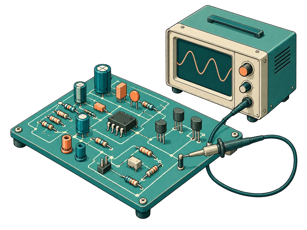
What you will learn
- Calculate voltage, current, power, loading, and component limits
- Solve nodal and Thevenin DC models and RC/RL time response
- Read phasor magnitude, phase, and first-order Bode plots
- Estimate diode, BJT, and MOS operating points with stated assumptions
- Design op-amp feedback and check swing, bandwidth, slew, and noise
- Prepare a schematic connection table and verify a low-voltage sensor amplifier and filter
Before you begin
These browser exercises use educational models; they do not compile or run HDL. To run the supplied source separately, follow the Digital Design Studio guide for your operating system and sign in when the operation requires it.
Installation and first launch ↗ · Downloads ↗Curriculum
- Voltage, current, power, and conservation
- Voltage is a difference, not a labelConcept
Choose a reference node, convert units, and calculate a resistor voltage.
- Current, power, and component limitsConcept
Distinguish charge flow from energy flow and check resistor dissipation.
- KCL and KVL make a circuit solvableConcept
Write consistent current and voltage equations for a divider.
- Check: a sign-consistent dividerCheck
Check the model, calculation, and interpretation before continuing.
- Nodal analysis, equivalents, and loading
- Solve a node connected to several sourcesConcept
Turn a circuit drawing into one node equation and audit branch currents.
- Thevenin equivalents preserve the load behaviorConcept
Replace a linear source network with an open-circuit voltage and resistance.
- Loading changes what you measureConcept
Calculate meter and amplifier input loading instead of assuming infinite impedance.
- Lab: predict and simulate a loaded dividerLab
Run a DC operating point and distinguish source current from load current.
- Stored energy and time response
- Capacitors connect voltage change to currentConcept
Use capacitance, charge, energy, and initial conditions consistently.
- Inductors connect current change to voltageConcept
Calculate an RL time constant and recognize current continuity.
- RC steps: initial value, final value, time constantConcept
Predict charging, discharge, and settling from the resistance seen by a capacitor.
- Check: capacitor loading and settlingCheck
Check the model, calculation, and interpretation before continuing.
- Phasors and frequency response
- Phasors describe a sinusoidal steady stateConcept
Use complex impedance while separating RMS, peak, and phase.
- Read magnitude and phase on a Bode plotConcept
Calculate a first-order corner, decibels, and meaningful test frequencies.
- Lab: connect a time constant to an AC cornerLab
Use the same circuit for transient and small-signal AC analyses.
- Check: RMS and a low-pass cornerCheck
Check the model, calculation, and interpretation before continuing.
- Diodes and transistor operating points
- A diode model must match the questionConcept
Use a constant-drop approximation while identifying its limits.
- BJT bias creates room for a small signalConcept
Estimate an emitter-degenerated operating point and small-signal gain.
- MOSFET bias and the limits of square-law modelsConcept
Separate threshold, overdrive, operating region, and incremental gain.
- Check: an inconsistent transistor biasCheck
Check the model, calculation, and interpretation before continuing.
- Operational amplifiers and feedback
- Negative feedback and the virtual-short conditionConcept
Explain why similar input voltages depend on a functioning feedback loop.
- An inverting amplifier uses a current balanceConcept
Calculate gain, input resistance, and a midrail-reference output.
- A noninverting stage preserves input polarityConcept
Design a gain around a reference and distinguish a buffer from a power source.
- Output range, bandwidth, and slew rate are separate limitsConcept
Test DC headroom and dynamic requirements before trusting an ideal gain.
- Filters and noise
- Choose low-pass or high-pass from the output nodeConcept
Design a first-order filter while accounting for source and load resistance.
- Lab: separate amplification from filteringLab
Simulate an educational gain stage plus RC pole and state what the model omits.
- Noise is a bandwidth-dependent error budgetConcept
Estimate resistor noise and combine independent contributions by root sum square.
- Check: signal bandwidth and noise bandwidthCheck
Check the model, calculation, and interpretation before continuing.
- Measurement, schematic setup, and a sensor capstone
- Tolerance and measurement uncertainty deserve separate budgetsConcept
Compute corner and gain extremes before choosing an acceptance band.
- From a connection table to a trustworthy schematicConcept
Draw and audit a low-voltage circuit without assuming a particular editor backend.
- Capstone lab: a low-voltage sensor amplifier and filterLab
Design, simulate, and explain a gain-11 sensor path with explicit physical limits.
- Final check: evidence and a capstone limitCheck
Check the model, calculation, and interpretation before continuing.